We use cookies in our website to give you the most relevant experience by remembering your preferences and repeat visits. By clicking "Accept All", you consent to our website's use of ALL cookies. However, you may click "Cookie Settings" to create a controlled consent or "Reject" to reject all except necessary cookies.
Cookie Settings
You have the choice whether to accept the use of cookies and may update your settings below. You can block cookies by activating the setting on your browser that allows you to refuse the setting of all or some cookies. However, if you use your browser settings to block all cookies, you may not be able to access all or parts of our Sites. Please review our Privacy Policy in the footer as well for more information on the cookies used.
Strictly Necessary
These cookies are necessary for the website to function and cannot be switched off in our systems. Without these cookies some services may not function.
Modular and Scalable Millimeter-Wave Patch Array Antenna for 5G MIMO and Beamforming
Published: 2020, EuMW
Abstract —Phased array antenna for 5G MIMO and beamforming using modular radiation element is proposed in this paper, which can be readily scaled up for massive MIMO applications. The rectangular probe-fed microstrip antenna is utilized as the radiation element in the array. The radiation pattern of phased array antenna remains intact after combination of beamforming have demonstrated scanning range over ±60 degrees in simulation. Two millimeter-wave phased array antennas with operating frequency of 28 GHz have been assembled and array elements tested to verify their performance. The proposed phased array structure demonstrates the flexibility of the array configuration, advantages of scalability, ease of assembly, and element failure correction, compared with conventional designs.
The new 5G wireless communication standard promises to provide a top data rate of up to 10 Gbps by using millimeter-wave (mm-wave) frequency spectrum at available bands, such as 28 GHz and 39 GHz within the designated FR2 spectrum. However, the path loss and the requirement for direct line-of-sight at mm-wave frequency bands is significantly higher than that of 4G bands presenting considerable challenges. The use of massive multi-input multi-output (MIMO) phased array antennas provides high directivity and allow multiple incoming/outgoing signals to improve spectral efficiency and provide significant contribution to increased data transfer rates. Moreover, further research into the beam-steering capability of phased array enables the communication system to continuously track mobile users.
Planar antenna has been widely used in mm-wave antenna systems due to its advantages of low profile, lightweight, low cost in fabrication, ease of integration with other components. In [1], patch antennas are integrated with SiGe beamformer chips to realize a mm-wave 5G 8×8 phased array at 39 GHz. Many types of phased array utilizing planar antennas have been developed for 5G MIMO communications. A seven-layer patch antenna using parasitic patch and coupling structure is utilized as antenna cell for a 5G phased array antenna is demonstrated in [2]. A leaf-shaped bowtie antenna fed with microstrip line detailed in [3] was used to form a 1×8 5G phased array for MIMO application at 28 GHz and 38 GHz. In [4], an 8-channel 1 dimensional beam steering patch array at 28 GHz using element of 1×16 linear array is proposed for 5G MIMO application with high gain and good cross-polarization separation. In [5], the 28 GHz 1×8 phased array using square patch element is studied, and the mutual coupling effect in a phased array is characterised.
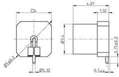
Fig. 1. SMPM connector, unit in mm, 18S102-40ML5 – Rosenberger [6].
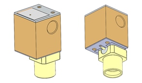
Fig. 2. Configuration of single patch element, SAM-2832830695-DM-LE.
Although many phased arrays for 5G MIMO have been proposed and developed, one thing is clear. It is still challenging and difficult to design and implement customized phased array for mm-wave 5G prototyping, especially massive or hybrid arrays with 64 elements or more. The stringent restrictions for spacing between antenna elements, as this is related to wavelength of operation and maximum steering angle, poses significant challenges for feeding network design for massive phased arrays. To solve this problem, we introduce the usage of commercially available mini-SPM (SMPM) connector implementations of which operates up to 65 GHz, as shown in Fig. 1, which enable us to feed each antenna element directly in an inline fashion allowing for a modular design.
In this paper, modular and scalable mm-wave phased array designs using uniform patch elements are presented. Each patch element is probe-fed with a SMPM connector at its bottom in an inline fashion, as shown in Fig. 2. Due to the reduced size of SMPM connector compared to traditional coaxial connectors, each patch element can be manufactured as a singular module. With these identical modules, we can form potentially massive phased arrays with various configurations, e.g., diamond array, hexagon array, octagon array, and so on with minimum additional effort and cost. To verify this concept, two rectangular arrays, i.e., 1×32 and 4×16, are designed, fabricated and assembled with identical patch elements resonating at 28 GHz. Their performances have been validated through test. It is noted that SMPM connectors can also be used for 39 GHz and higher modular phased array with reduced theoretical maximum scanning angle of ±67 degrees, instead of ±90 degrees.
A. Radiation Element Design The proposed radiation element is composed of four parts in the module assembly, i.e., the probe-fed patch antenna circuit, ground plane block, SMPM connector attachment board, and SMPM connector. A short section of coax cable connects the feeding point of patch antenna on the top of the antenna with the connector pin at the bottom, and 50-ohm impedance is maintained along this connection. Due to the high loss of substrate in mm-wave, substrate with lower loss tangent is preferred to maintain the radiation efficiency of antenna element. Another consideration is the thickness of substrate material. Though thicker substrate will enhance the operating bandwidth of patch antenna, it will in turn increase the substrate loss and surface wave in propagation as well. For optimal performance, both of patch antenna and SMPM connector footprint are fabricated on Rogers RT/Duroid 5880 substrate with dielectric constant of 2.2, loss tangent of 0.0009, and thickness of 0.254 mm.
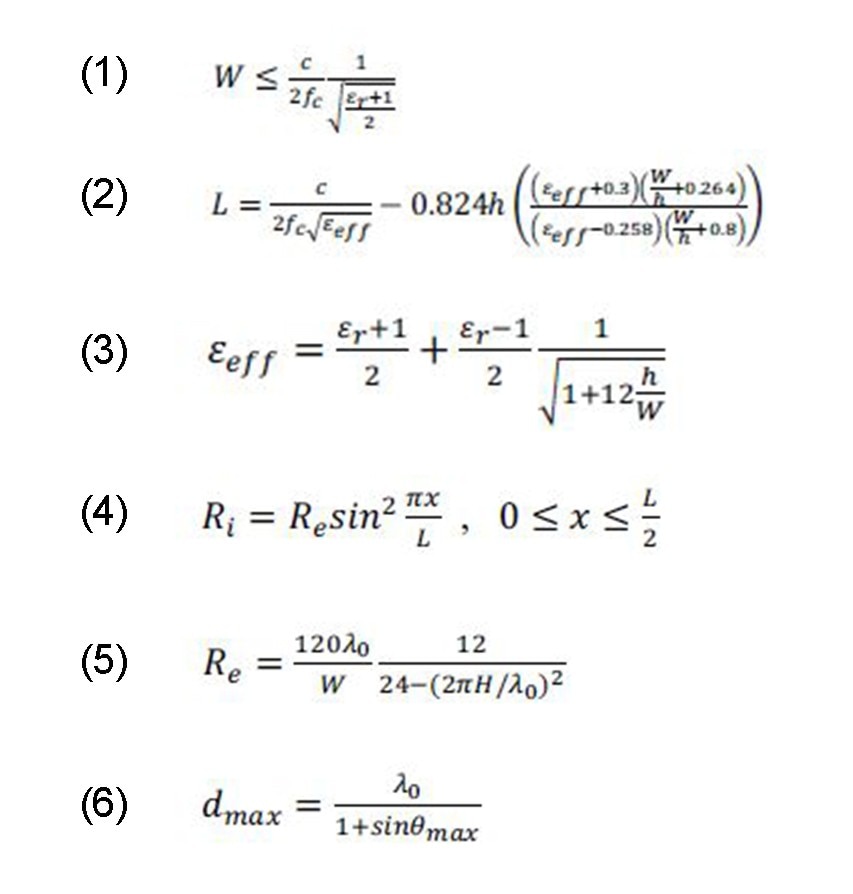
The width W of the patch element can be determined with the equation below [7], where c is the speed of light, fc indicates the operating frequency, and εr denotes the substrate dielectric constant. The patch length L can be determined using equation 1 [7], where c is the speed of light, fc indicates the operating frequency, and εr denotes the substrate dielectric constant. The patch length L can be determined using equation 2 [7], where h is the substrate thickness, εeff denotes the effective dielectric constant of substrate, which is The next step is to find the probe feeding point, where the rectangular patch has an impedance of 50 Ω. The impedance from the patch center to the edge can be estimated as where Ri is the input impedance at the feeding point, Re is the input impedance at patch edge, λ0 is the free-space wavelength at center frequency. After the required patch parameters are estimated with aforementioned equations, the patch design can be optimized with full-wave simulator for optimal performance.
B. Mechanical Design Consideration In a phased array, the antenna element must be properly spaced to avoid grating lobes in a combined beam after beamforming. The relation between maximum spacing and wavelength of operation can be described as equation 6, where dmax indicates the maximum spacing between elements, θmax indicates maximum beam angle after beamforming. To realize scanning angle at ±90 degrees, the antenna element spacing has to be λ0/2. At 28 GHz and 39 GHz, they are 5.4 mm and 3.9 mm, respectively. For the 28 GHz phased array, SMPM connector is used due to its smaller size compared with its counterparts such as 2.92mm (K) connector. The drawing of SMPM connector 18S102-40ML5 from Rosenberger, Fig. 1 [6]. It has a planar dimension of 4 mm×4 mm, which is smaller than maximum grid size λ0/2×λ0/2 at 28 GHz. SMPM connector is qualified for various configurations phased array design at 28 GHz.
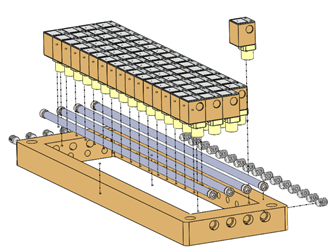
The assembly illustration of the 4×16 phased array is presented in Fig. 3. All patch elements are placed side by side and confined by to the frame. Four rods go through the mounting holes of four rows of modules. Set screws for each column of modules are used to secure the assembly.
This rectangular array can be readily scaled up to a massive phased array with more than 64 radiation elements. The assembly in Fig. 3 applies to other configuration as well, such in a diamond, with a properly designed frame. N×1 or 1×N configurations at 28 GHz are also easily configured in line with common 4G antenna deployments [8]. This design is friendly to production and has the advantages of low cost, ease of assembly, element failure correction and scalability.
Fig. 5. Simulated and measured radiation pattern of the patch element SAM- 2832830695-DM-LE at (a) E-plane, (b) H-plane.
Fig. 6. Fabricated phased array 1×32 array SAM-2832830695-DM-L1-32C-1 (a) front, (b) back, and 4×16 array, SAM-2832830695-DM-L1-64C (c) front, (d) back
Fig. 7. Simulated patterns at 28 GHz of 1×32 array when scanning angles are at boresight, ±30 degrees, and ±60 degrees.
Fig. 8. Simulated patterns at 28 GHz of 4×16 array, SAM-2832830695-DML1- 64C, when beam steered to (a) 30 degrees at E-plane, and (b) 60 degrees at H-plane.
III. FABRICATION AND EXPERIMENTAL RESULTS
A. Single Antenna Element Test Results Single antenna element resonating at 28 GHz has been designed and fabricated. The return loss and radiation pattern for single module have been sampled to verify the performance. The physical dimensions of one module is 5.3 mm×5.3 mm×9.3 mm, which corresponds to electrical size of 0.5λ0×0.5λ0×0.9λ0. Simulated and measured return loss and pattern of the single patch element are shown in Fig. 4 and Fig. 5, respectively. The simulated 10-dB return loss bandwidth is around 0.9 GHz from 27.5 GHz to 28.4 GHz, which corresponds to a fractional bandwidth of 3.2%. The measured half-power beam-width of this module is 78 degrees for Eplane and 65 degrees for H-plane. The performance of antenna element is validated through tests. Note that, the radiation pattern of single antenna element in a phased array is distorted due to edges of finite ground plane, as well as mutual couplings of other elements in the array. It is recommended to qualify each antenna element before assembly in production. All the simulation results are acquired with full-wave electromagnetic simulator CST Microwave.
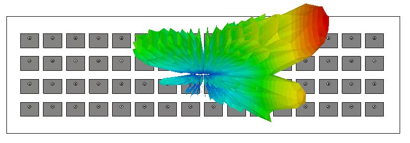
Fig. 9. Simulated 3-D patterns at 28 GHz of 4×16 array, SAM-2832830695- DM-L1-64C where beam is steered to 30 degrees at and 60 degrees at H-plane simultaneously.
B. Beam Steering of Phased Arrays Two arrays using the identical antenna element have been assembled, as shown in Fig. 6. The 1×32 array in linear configuration has a physical dimension of 180.3 mm×12.7 mm×10.9 mm; the 4×16 array in rectangular configuration has a size of 101.6 mm×33 mm×10.9 mm. Two customized frames are fabricated to hold the elements together. Each patch element is in broadside polarization to reduce the surface wave coupling [5]. Fig. 7 shows the simulated H-plane patterns of the 1×32 array at 28 GHz, when the array elements are excited with signals in progressive linear phase difference. When phase differences between adjacent ports are 0 degrees, ±90 degrees, and ±155.9 degrees, the scanning angles in H-plane will be 0 degrees, ±30 degrees, and ±60 degrees, respectively. Fig. 8 shows the simulated radiation patterns at 28 GHz of the 4×16 array, when the beam is steered to 30 degrees at E-plane and 60 degrees at H-plane, respectively. The 3-D radiation pattern is presented in Fig. 9 when the array is steered to 30 degrees at E-plane and 60 degrees at H-plane simultaneously. Both 1×32 and 4×16 phased arrays have demonstrated good beam-steering capability with over ±60 degrees scanning ranges in simulation.
IV. CONCLUSION
In this paper, modular and scalable phased array using modular elements is proposed for 5G Massive MIMO applications. The utilization of SMPM connectors enables modular configuration concept and minimization of phased array design. The details of design for the single patch element and mechanical considerations in array assembly are provided. Modular patch elements resonating at 28 GHz has been designed and fabricated and tested. Two phased arrays, i.e., 1×32 and 4×16 arrays, have been assembled with the modular 28 GHz patch elements. Both phased arrays have demonstrated scanning range over ±60 degrees in simulation and will be validated via next phase testing. Modular phased arrays with reduced theoretical scanning angle past 39 GHz are also producible. The modular and scalable design provides a low-cost and flexible solution to the anticipated continuation of mm-wave 5G Massive MIMO related research and product development. This innovative design eases realization of various array size and configurations in a low cost and reduced cycle time manner.
REFERENCES
[1] Y. Yin, S. Zihir, T. Kanar, and G. M. Rebeiz, “A 37-42 GHz 8x8 Phased-Array for 5G Communication Systems with 48-50 dBm EIRP,” IEEE MTT-S International Microwave Symposium (IMS), June. 2019. [2] J. Li, Z. Yang, Y. Li, X. Sun, J. Lv, and W. Zhong, “Research on Millimeter Wave Phased Array Antenna for 5G Communication,” IEEE International Conference on Electronic Information and Communication Technology (ICEICT), Jan. 2019. [3] N. O. Parchin, M. Shen, and G. F. Pedersen, “End-fire phased array 5G antenna design using leaf-shaped bow-tie elements for 28/38 GHz MIMO applications,” IEEE International Conference on Ubiquitous Wireless Broadband (ICUWB), Oct. 2016. [4] S. Krishna, G. Mishra, and S. K. Sharma, “A series fed planar microstrip patch array antenna with 1D beam steering for 5G spectrum massive MIMO applications,” IEEE Radio and Wireless Symposium (RWS), Jan. 2018. [5] X. Chen, M. Abdullah, Q. Li, J. Li, A. Zhang, and T. Svensson, “Characterizations of Mutual Coupling Effects on Switch-Based Phased Array Antennas for 5G Millimeter-Wave Mobile Communications,” IEEE Access, Vol. 7, pp. 31376-31384, March. 2019. [6] “18S102-40ML5 - Mini-SMP - Rosenberger Asia Pacific Electronic Co., Ltd.,” Rosenberger. [Online]. Available: https://www.rosenbergerap.com/product/show/3066.aspx. [Accessed: 12-Feb-2019]. [7] Jun zhang and KeCheng Liu, Microstrip antenna theory and Engineering, National Defense Industry Press, China, 1988. [8] Björnson Emil, J. Hoydis, and L. Sanguinetti, Massive MIMO networks: spectral, energy, and hardware efficiency. Hanover, MA: Now Publishers, 2018.