Contactless Waveguide Flange Enables Faster Measurements
Published: August 2024, Microwave Journal
Applications continue to expand for mm-wave and THz frequencies in aerospace, military, industrial, and consumer markets. As a result there is increasing demand for faster and more reliable methods of testing waveguide components. At these frequencies, rectangular waveguide is commonly used to carry signals between components and subassemblies. Standard and non-standard flanges are the predominant means of connecting waveguide sections. When they are joined, precisely machined flanges provide continuous electrical contact around the mated waveguide openings.
Unfortunately, measurements of waveguide components are easily compromised by poor connections. Common problems include waveguide cocking, which occurs when flange surfaces are not perfectly parallel. Repeated connections can also degrade flanges on waveguide test equipment such as VNA frequency extenders, power meter heads, frequency converters, and calibration standards. Periodic replacement of expensive test system components is required to ensure accuracy and repeatability over time.
Inadvertent gaps and surface damage may be minimized by carefully and evenly tightening the screws that provide mechanical contact between the waveguide flanges. This task requires substantial training and skill to be performed correctly. When done repeatedly in a production environment, this work also requires high levels of endurance and discipline. Ultimately, the use of traditional waveguide flanges in high-frequency test systems limits how quickly and reliably components can be qualified and sorted in manufacturing operations.
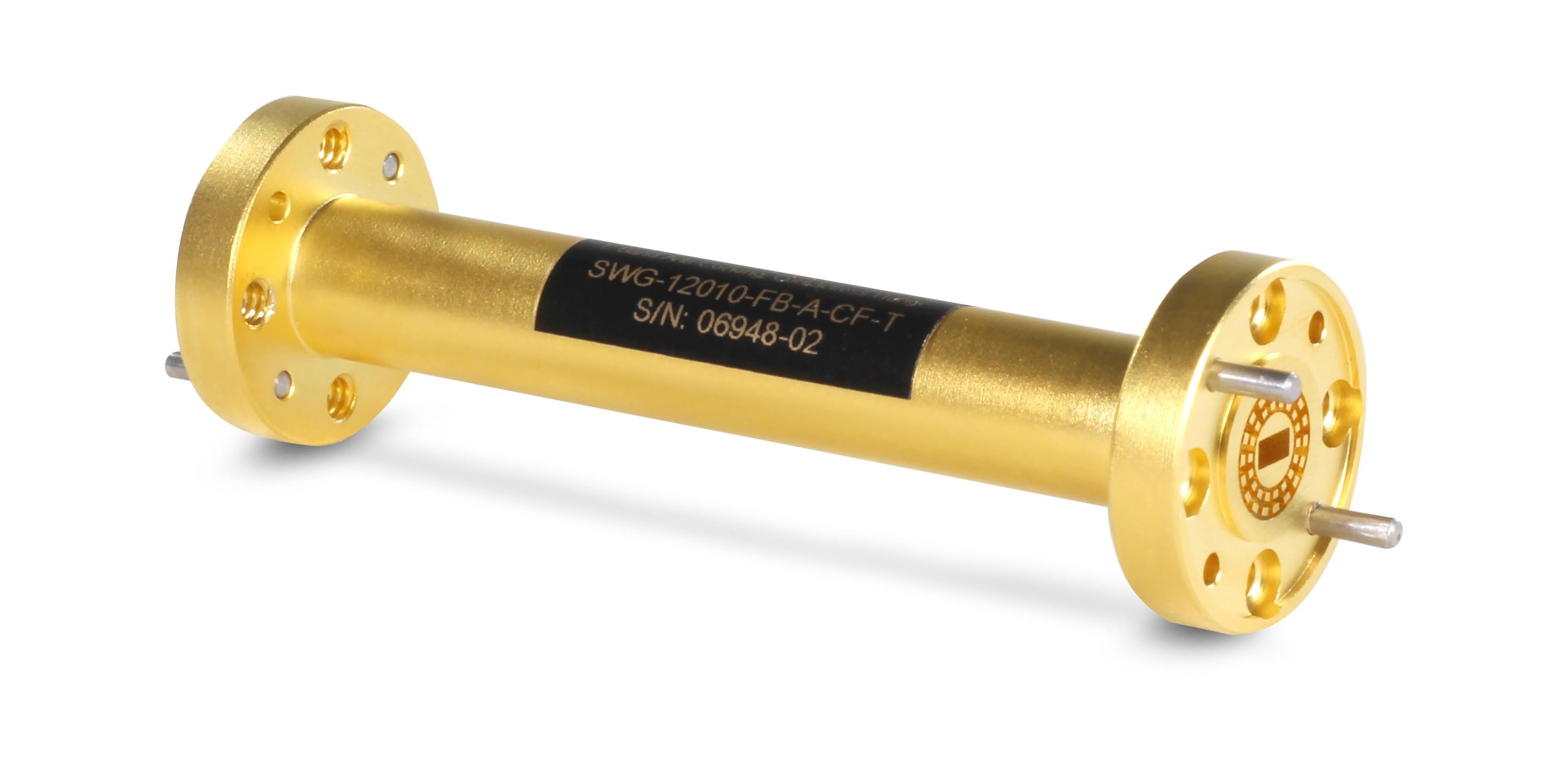
A proposed Contactless Waveguide Flange (CWF) can be used without inserting the flange screws that are mandatory with conventional flanges. When used with streamlined test fixtures, the CWF enables much faster mm-wave and THz measurements while maintaining satisfactory levels of accuracy and reliability.
The construction of waveguide-based systems requires the physical interconnection of components, commonly achieved through the use of standard waveguide flanges and screws. One of the challenges associated with high-frequency (mm-wave and THz) devices is a strict mechanical requirement for good electrical contact between waveguide flanges. The flanges must be tightly connected to each other to avoid mechanically induced interface mismatches.
Small gaps between the mating flanges can lead to power leakage and poor return loss, causing unreliable and inaccurate measurements [1]-[2]. Repeatedly attaching and detaching waveguide flanges degrades their quality and performance over time. This activity also slows down testing, which can be detrimental in areas where speed is a priority. The CWF was developed to preserve the electrical and mechanical integrity of both the Device Under Test (DUT) and the test system, without sacrificing measurement results.
Theory of Operation
The CWF employs gap waveguide technology while applying the well-known principle of operation of the choke flange. The CWF choke is a recessed ring engraved into the flange at a nominal depth of λg/4 and a distance λg/4 from the waveguide walls, where λg is the guide wavelength.
Gap waveguide technology has been thoroughly investigated and used previously in the design of antenna array feeding structures and other passive components [3]. These studies demonstrate that when a perfect magnetic conductor (PMC) plate and a perfect electric conductor (PEC) plate are positioned such that they are parallel to each other and the distance between them is less than λ0/4, where λ0 is the wavelength of the operating frequency in air, a cut-off condition is created. As a result, parallel-plate transmission modes cannot propagate between the plates.
Further, it has been shown that textured surfaces formed by metallic pins attached to a ground plane can exhibit the electrical characteristics of a PMC, thus forming an Artificial Magnetic Conductor (AMC) over a limited range of frequencies. Often referred to as a “bed of nails substrate” such an arrangement may be used to suppress dielectric surface waves in planar antenna structures.
In the CWF, the choke ring is populated with concentric rings of small pin-like structures to realize a high-impedance AMC surface that approximates a PMC plate. Conversely, the mating surface on a conventional flange is flat, approximating a PEC plate.
It employs a standard waveguide flange that is modified by adding two concentric rows of pins that fill a choke ring engraved around the waveguide opening. The inner-most metal surface that surrounds the waveguide opening has a nominal width of about λg/4 across the opening’s two longer sides. Its purpose is to transform an open circuit into a short circuit at the waveguide opening. Along the two shorter sides of the waveguide opening the inner metal surface is thinner to increase the connection bandwidth [4]-[5].
Design Considerations
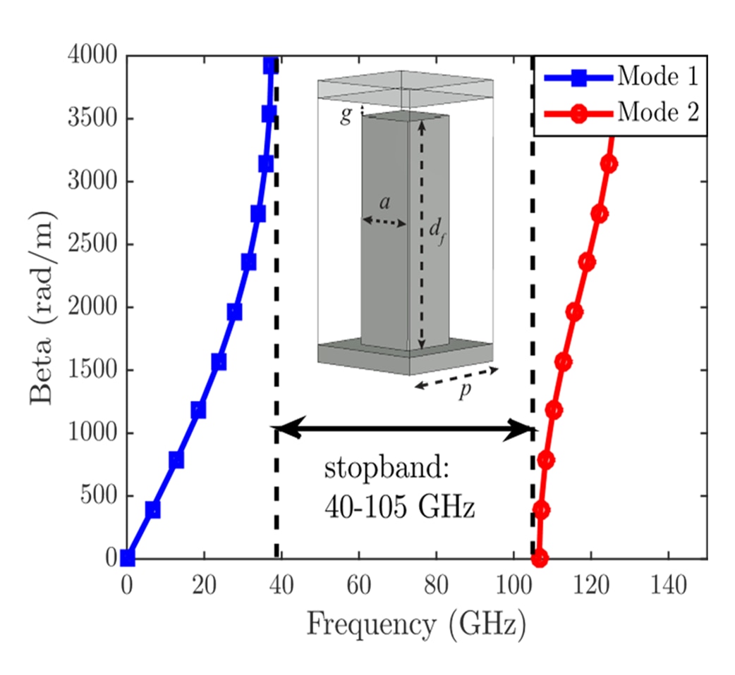
Fig. 2. The dispersion diagram for an infinite periodic pin unit cell shows a stop band of 40 to 105 GHz.
The pin width and the distance between the pins affect the stop band of the combined AMC and PEC surfaces. However, the stop band is also affected by the pin height and the resulting thickness of the air gap between the AMC and PEC surfaces. The bandwidth increases as the gap between the two surfaces decreases. The stop band also moves toward lower frequencies as the height of the pins increases, following an inverse relationship [4].
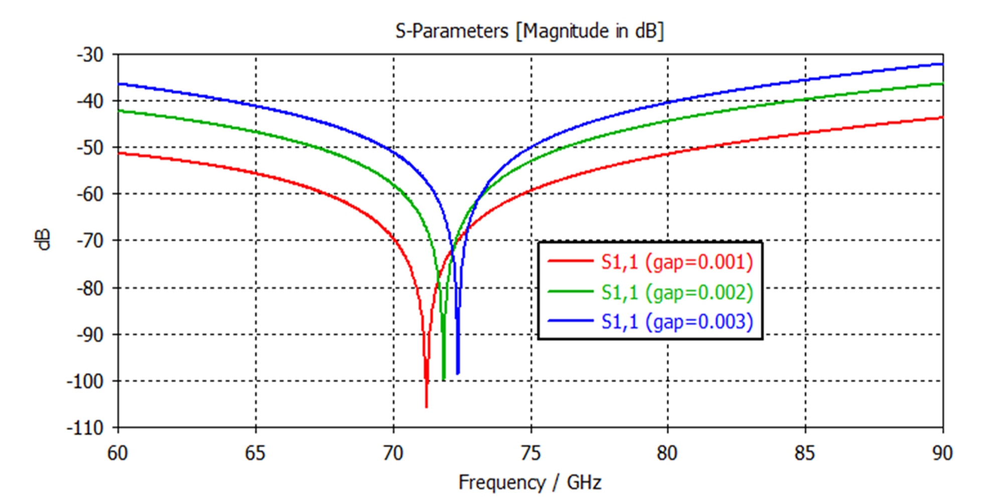
Fig. 3. Simulated S11 for different gap sizes predicts the return loss caused by reflections at the waveguide flange interface.
The stop band covers frequencies from 40 to 105 GHz, including the entire E-band (60 to 90 GHz). Unlike previous designs [7]-[11], the current design combines the functions of a choke flange design [6] with gap waveguide technology to suppress signal leakage and minimize reflections. The two rows of pins form a circular pattern to ease the mechanical design and fabrication of the pins. The pins form an AMC surface that creates a parallel-plate cut-off condition at the junction between waveguide flange surfaces, and in this way reduces signal loss and reflection. The present E-band gap adapter design has a fixed air gap (g) of 3 mils, although smaller gaps can be used to achieve better performance.
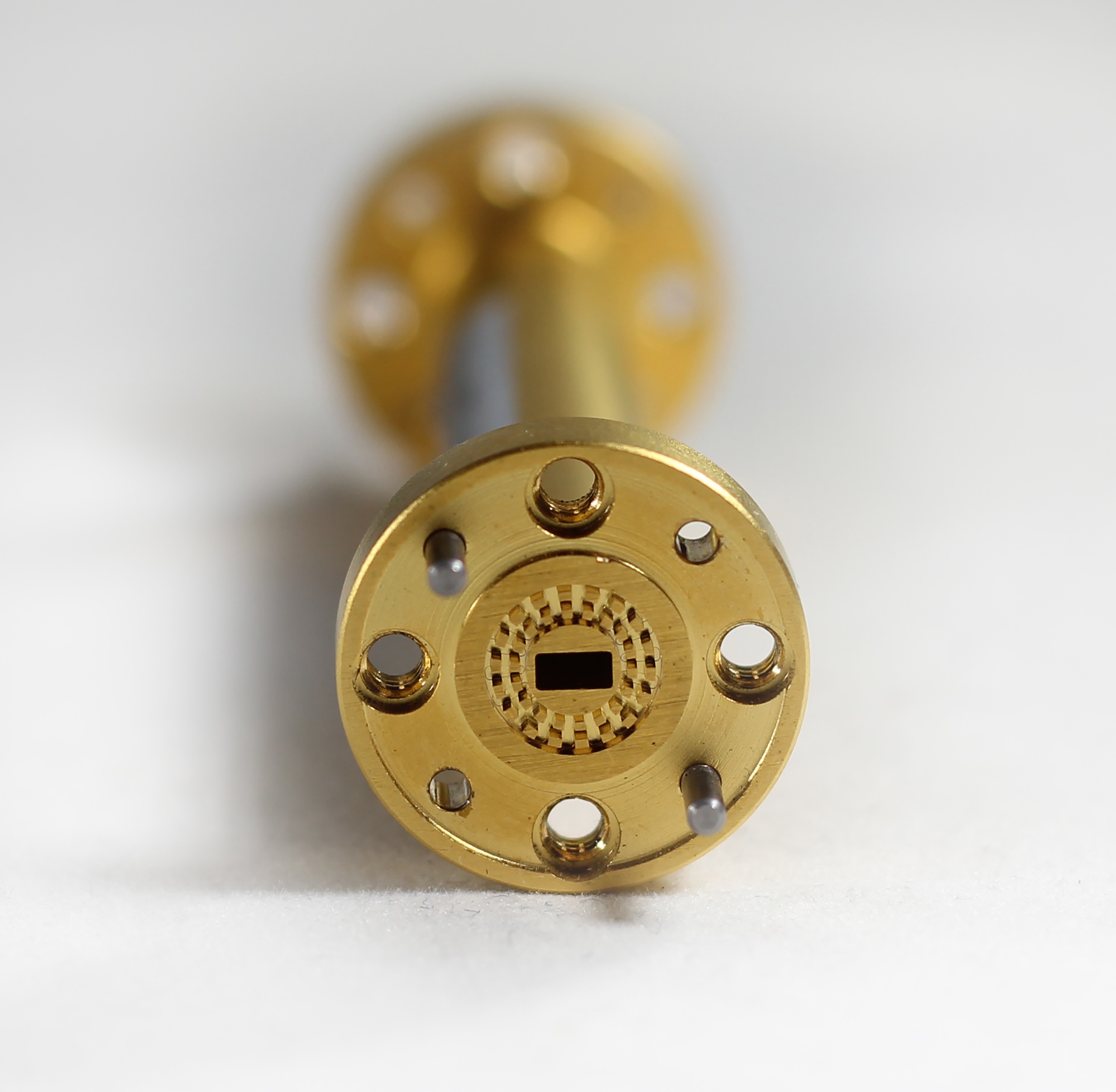
Fig. 4. The front face of the contactless flange has an outer rim that is 3 mils thicker than the pin array to prevent damage to the pin surfaces.
The CWF design was refined by performing repeated simulations and iterations. The process involves necessary trade-offs between electrical performance and manufacturability. In the present design, S11 was examined for different gaps between the waveguide flanges. From 60 to 90 GHz, expected return loss is better than -30 dB for a 3-mil gap and -40 dB for a 1-mil gap (Fig. 3). The simulated results indicate that good electrical performance is achievable without requiring any physical contact between the flanges.
The rim surrounding the waveguide opening has the same height as the pins. Its short walls are 14 mils thick while its long walls are nominally 45 mils thick across the longer dimension of the waveguide opening. Another rim with radial thickness of 47 mils surrounds the pin array that forms the AMC surface. This external rim protects the pin surfaces from damage. It also determines the minimum gap between the AMC and PEC surfaces.
Guide pins are included to ensure proper alignment between the CWF and the conventional flange in adherence to standard flange definitions. By eliminating the need for screws, measurements can be performed considerably faster since the flanges only need to be aligned and pushed together.
Measured Results
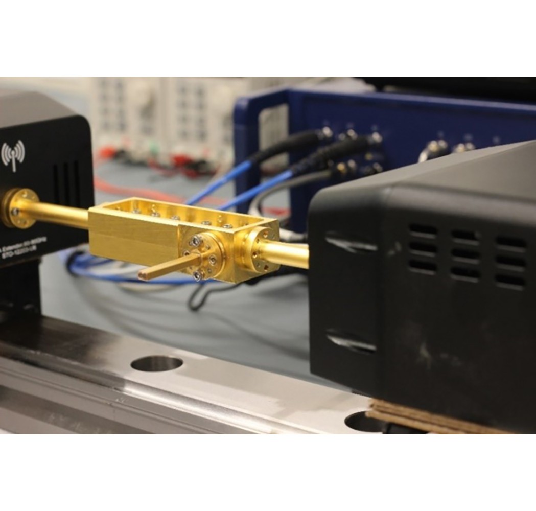
Fig. 5. The CWF can be used with a pair of VNA extenders that slide on rails. The DUT is easily inserted and removed while test port alignment is maintained.
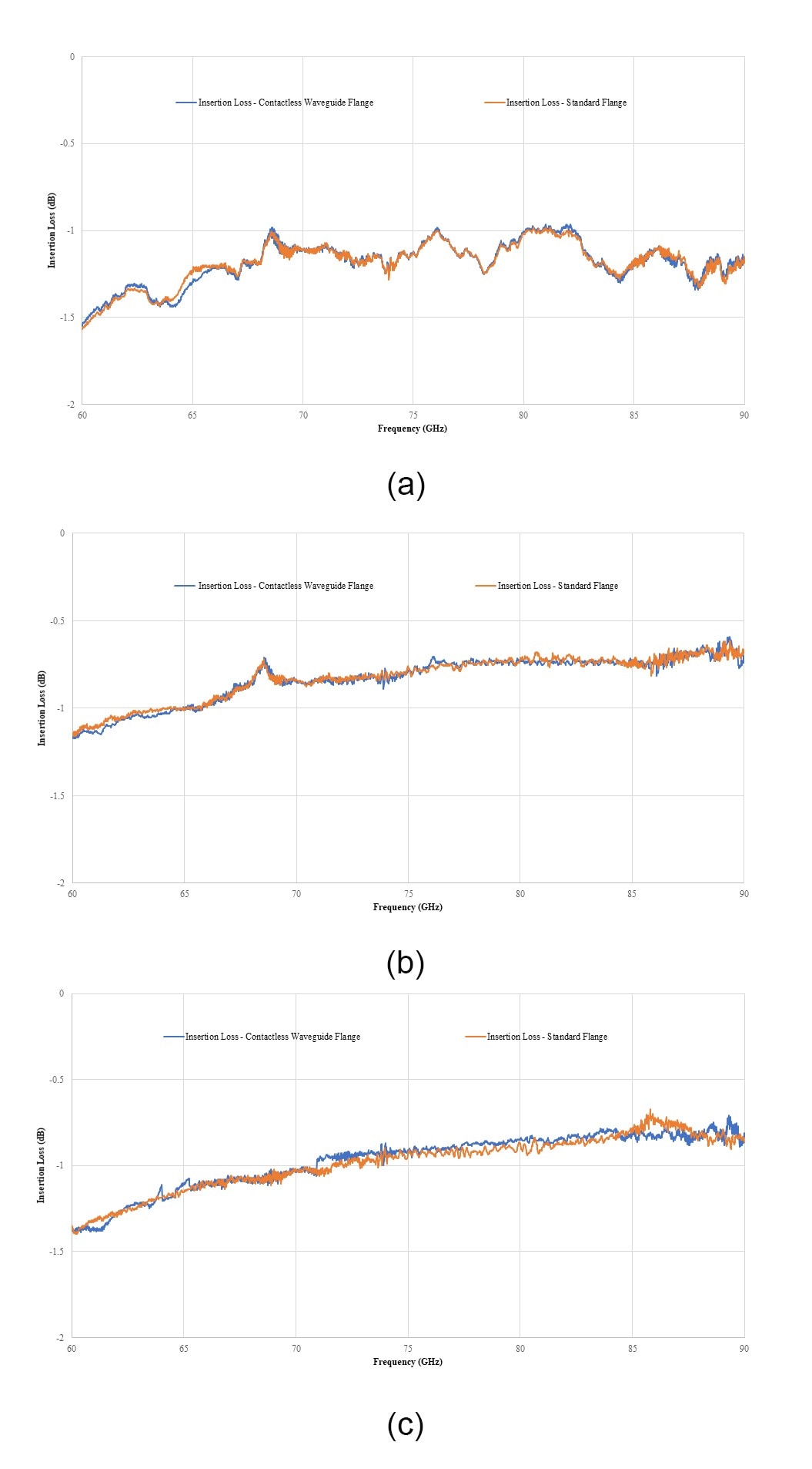
Fig. 6. Measured insertion loss for an E-band isolator (a), a directional coupler (b), and another directional coupler (c).
The E-band CWF was used to measure the insertion loss of an isolator and two different directional couplers. The results were then compared with those obtained from measurements using conventional flanges as shown in figure 6 (a), (b) and (c). The results show minimal differences (less than 0.1 dB) between the two setups. The data demonstrate that the CWF can achieve reliable measurement results. The insertion loss measurements were repeated five times and the results were the same in all instances.
Additional CWF designs are being developed for waveguide sizes ranging from WR-28 to WR-05, covering frequencies from 26.5 to 220 GHz. It is expected that increasing demand for waveguide components in greater quantities will motivate more manufacturers to adopt the CWF in their test systems for increased productivity and reduced operator fatigue in high-volume production environments.
REFERENCES
[1] A. R. Kerr, “Mismatch caused by waveguide tolerances, corner radii, and flange misalignment,” Nat. Radio Astronomy Observatory, Charlottesville, VA, USA, Tech. Rep. Electronics
[2] Division Technical Note No. 215, 2010. [Online]. Available: https://library.nrao.edu/public/memos/edtn/EDTN_215.pdf
[3] P.-S. Kildal, "Three metamaterial-based gap waveguides between parallel metal plates for mm/submm waves", 3rd European Conference on Antennas and Propagation, 2009. EuCAP 2009. Berlin, Germany, 2327 March 2009.
[4] E. Rajo-Iglesias and P.-S. Kildal, “Numerical studies of bandwidth of parallel-plate cut-off realised by a bed of nails, corrugations and mushroom-type electromagnetic bandgap for use in gap waveguides,” IET Microwaves, Antennas & Propagation, Volume 5, Issue 3, 21 February 2011, pp. 282-289
[5] E. Pucci and P.-S. Kildal, “Contactless non-leaking waveguide flange realized by bed of nails for millimeter wave applications,” in Proc. 6th Eur. Conf. Antennas Propag. (EUCAP), May 2012, pp. 3533–3536
[6] R. Naruse, H. Saito, J. Hirokawa, and M. Zhang, “Non-contact wavefeed with choke-flange waveguide at the development section of the expansion antenna for small satellite,” IEICE, Tokyo, Japan, vol. 114, no. 194, pp. 77–82, Tech. Rep. SANE 2014-61, Aug. 2014.
[7] Xiang Chen, Wanzhao Cui, etc. “Low Passive-Intermodulation Contactless Waveguide Adapter Based on Gap Waveguide Technology,” 13th Eur. Antennas Propag. Conf., 2019.
[8] P.-S. Kildal, E. Alfonso, A. Valero-Nogueira, and E. Rajo-Iglesias, “Local metamaterial-based waveguides in gaps between parallel metal plates,” IEEE Antennas Wireless Propag. Lett., vol. 8, pp. 84–87, Apr. 2009
[9] H. Li, A. Arsenovic, J. L. Hesler, A. R. Kerr, and R. M. Weikle, “Repeatability and mismatch of waveguide flanges in the 500–750 GHz band,” IEEE Trans. Terahertz Sci. Technol., vol. 4, no. 1, pp. 39–48, Jan. 2014.
[10] Dongquan Sun, Zhenhua Chen, and Jinping Xu. “Flexible rectangular waveguide based on cylindrical contactless flange,” Electron Lett., vol. 52, no. 25, pp. 2042-2044, Dec 2016.
[11] Dongquan Sun and Jinping Xu. “Real Time Rotatable Waveguide Twist Using Contactless Stacked Air-Gapped Waveguides,” Microw. Wirel. Compon. Lett. vol. 27, no. 3, pp215-217, March 2017.